Design and Study of a Wide-Band Printed Circuit Board Near-Field Probe
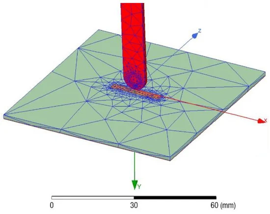
Magnetic near-field probes (NFP) represent a suitable tool to measure the magnetic field level from a small electromagnetic interference (EMI) source. This kind of antenna is useful as a magnetic field probe for pre-compliance EMC measurements or debugging tasks since the user can scan a printed circuit board (PCB) looking for locations with strong magnetic fields. When a strong H-field point is found, the designer should check the PCB layout and components placement in that area to detect if this could result in an EMI source. This contribution focuses on analyzing the performance of an easy-to-build and low-cost H-field NFP designed and manufactured using a standard PCB stack-up. Thereby, the frequency range and sensitivity of the NFP-PCB are analyzed through a Finite Element Method (FEM) simulation model that makes it possible to evaluate its sensibility and effective frequency range. The numerical results obtained with the FEM models are validated against measurements to verify the design and performance of our NFP. The FEM model reproduces the experimental procedure, which is used to evaluate the performance of the NFP in terms of sensitivity by means of the simulated near-field distribution. The NFP-PCB has almost a flat response from 180 MHz to 6 GHz, with an almost perfect concordance between numerical and experimental S21 results. The numerical results show an average transmission loss of −27.9 dB by considering the flat response bandwidth, whereas the experimental one is −29.7 dB. Finally, the designed NFP is compared to two high-quality commercial probes in order to analyze its performance.